EPD Develops First CMOS Pixel Sensor Prototype for CEPC
Scientists from IHEP's Experimental Physics Division (EPD) have developed the first pixel sensor prototype based on the 180 nm Complementary Metal–Oxide–Semiconductor (CMOS) imaging sensor process. This represents significant progress in the key technology of the micro-vertex detector, the core component for the detector at the Circular Electron Positron Collider (CEPC).
CMOS pixel sensors allow integration of the sensing element and its readout electronics on the same silicon substrate, which make them attractive for charged particle tracking. The CEPC micro-vertex detector, located closest to the e+e- interaction point, will use state-of-the-art pixel technologies that provide high spatial resolution, are capable of high readout speed and adequate radiation hardness, and feature low power consumption.
The first prototype sensors, named JadePix 1, have been characterized with radioactive resources, and recently by the electron test beam at DESY in Hamburg, Germany. Preliminary results show that spatial resolutions better than 5 μm and 3.5 μm can be achieved for pixel sizes of  and
and  , respectively. More importantly, there is no significant resolution degradation after exposure to neutron irradiation up to 1013 1 MeV neq/cm2.
The proposed Circular Electron Positron Collider (CEPC) aims at measuring Higgs properties with high precision and probing new physics beyond the Standard Model of particle physics. The CEPC Study Group has completed the conceptual design report (CDR) for the e+e- collider, and is completing the CDR for the detector. The group is pursuing an R&D program involving technologies critical for realizing the CEPC.
IHEP's EPD division initiated the R&D project to develop the novel CMOS pixel sensors. The advanced silicon tracking detectors and associated electronics have been the focal research direction at EPD. The division has been actively participating in several international projects, including the ATLAS Inner Tracker Upgrade, to gain design and construction experience for silicon detectors.
In addition, the division has developed pixel detectors for X-ray imaging. These detectors will soon be deployed at various stations of the High Energy Photon Source (HEPS), which will be constructed near Beijing. Meanwhile, EPD is pushing forward pixel detector R&D for the CEPC using both CMOS and SOI technologies. The goal is to design a fully functional pixel sensor and construct a larger scale prototype detector in near future.
This R&D project has been jointly supported by the State Key Laboratory of Nuclear Detection and Nuclear Electronics, the IHEP Innovation Fund and Yifang Wang's science studio.

JadePix 1 prototype sensor (Image by IHEP)
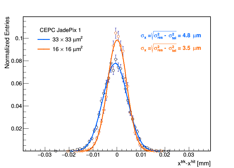
position resolutions obtained with electron test (Image by IHEP)
Contact Information
Mr. Guo Lijun
ljguo@ihep.ac.cn