Scientists from IHEP have successfully developed an engineering prototype based on through-silicon-via technology (TSV), which significantly reduces the module gap and improves the low-energy X-ray response. The achievement indicates that IHEP has reached the top domestic level in the design, technology and system integration of advanced X-ray pixel array detectors.
All the key technologies and advanced processes have been localized, and the detector performance is comparable to international mainstream products.
TSV technology is an advanced high-density packaging technology. It forms micropores through deep silicon etching, deposition of the insulating/barrier/seed layer, deep hole filling, chemical mechanical polishing, thinning, pad preparation and redistribution process technologies to achieve vertical electrical interconnection on chips.
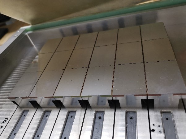
After more than a year in development and experimentation, the R&D team successfully reduced the gap between the modules from 9 mm to 2.5 mm. The detector is composed of 18 modules, which are spliced in a 3×6 manner. Each module has a pixel array of 208×288 with a 150 μm×150 μm pixel size.
The team will continue to promote the progress of silicon pixel detectors domestically. The technology for such detectors will improve the competitiveness of synchrotron radiation light sources in the future.
Meanwhile, the advanced technology involved in this project has the potential to be widely used in other fields, such as X-ray computed tomography, proton CT imaging in proton therapy, and space imaging detection.
This project is supported by the High Energy Photon Source (HEPS), the Platform of Advanced Photon Source Technology R&D (PAPS), the National Natural Science Foundation of China and the State Key Laboratory of Nuclear Detection and Nuclear Electronics.

3×6 TSV modules of the Engineering Prototype

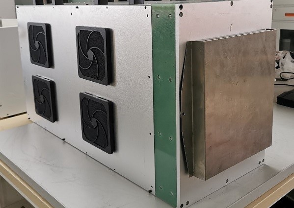
Engineering Prototype

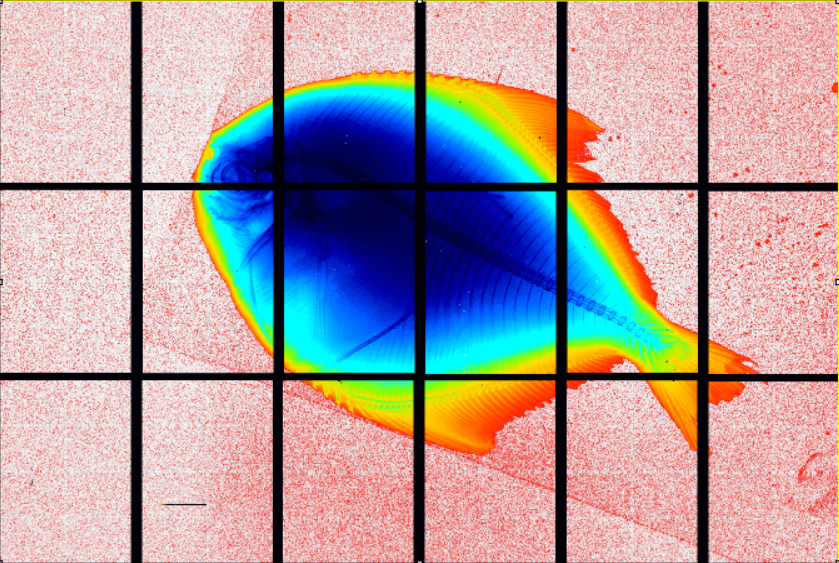
X-ray image of a fish
