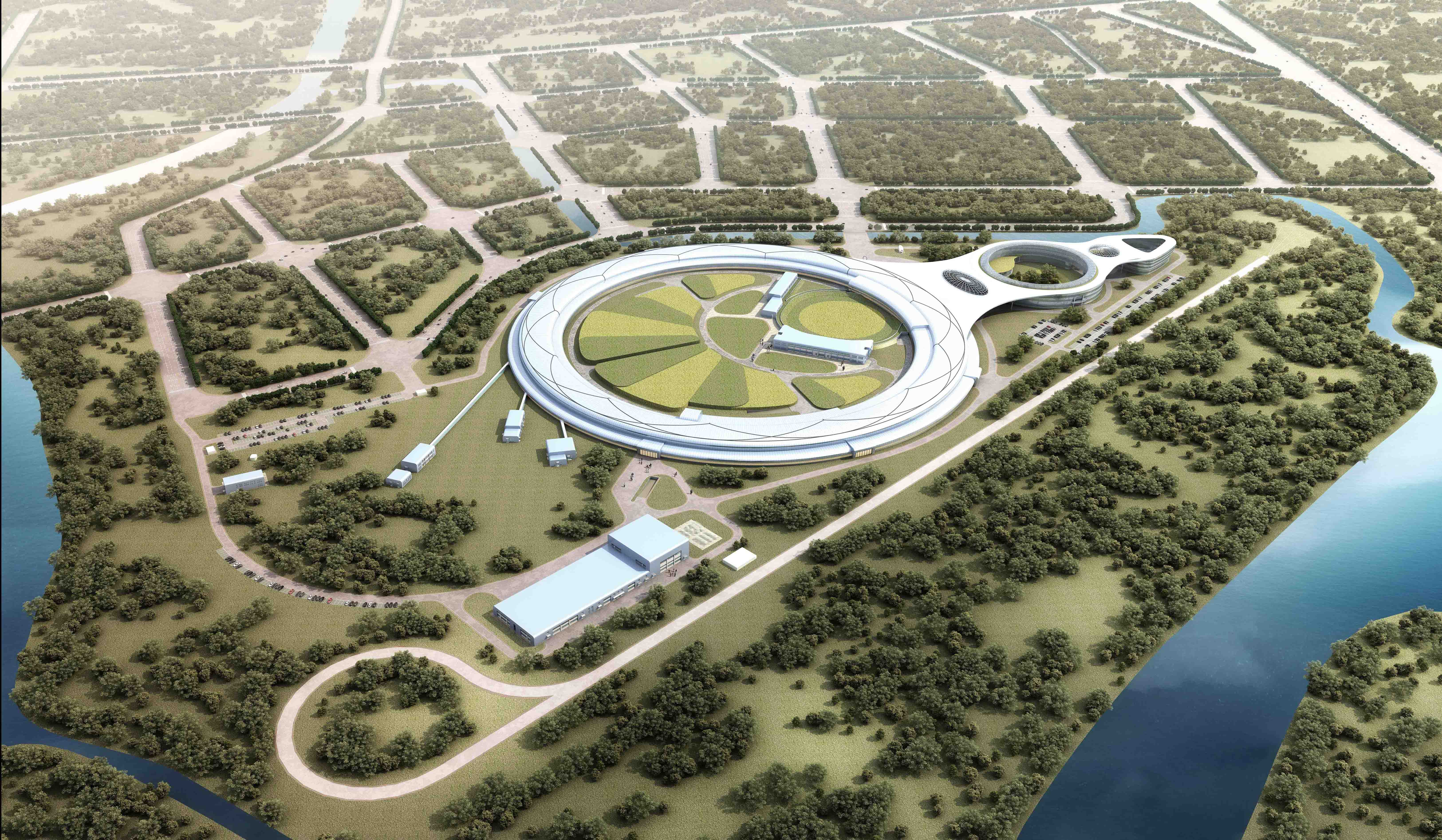
The circumference of the HEPS storage ring is 1360.4 m. The lattice takes a modified hybrid seven-bend achromat (7BA) design, in which some bending magnets with reversed bending angles and longitudinal gradients will enable the electron beam to reach an ultralow natural horizontal emittance of smaller than 60 pm.rad [1]. Forty-eight six-meter-long straight sections, with alternating high and low beta ones, are designed for generating the brilliant X-ray with a brightness of more than 1 × 10²² photons/s/mm2/mrad2/0.1% BW.
In Phase I, 14 beamlines will be constructed with 13 from insertion devices and one from the bending magnet. Feature beamlines will take advantage of the ultralow emittance to focus X-rays into a probe spot smaller than 10 nm with more than two orders of magnitude higher flux, and generate unprecedented coherent flux for coherence X-ray experiments. This high-energy machine could also provide a high-energy X-ray up to 300 keV for industrial applications. Among the Phase I beamlines, there are three long beamlines extending out of the experimental hall with a maximum length of 350 m. As the beamline construction will start after the infrastructure is finished, the optimization of beamline design will continue until 2021.
Prior to the HEPS project, an R&D project was launched in 2016 as part of the key technologies' preparation for HEPS. The output of the R&D project includes high-gradient quadrupoles, a small-aperture vacuum chamber with non-evaporable getter coating, and high-precision power supplies. A prototype of the cryogenic permanent magnet undulator has been set up with a period as short as 13.5 mm and PrFeB as the magnet material. For R&D of beamline technologies, a new type of long trace profiler—“FSP”—has been developed, whose self-comparison accuracy for curved surfaces is up to 30 nrad in RMS, comparison accuracy with interferometer is up to 0.1 nm in RMS, and the elliptically bent mirror achieves bending accuracy up to 130 nrad. Different prototype monochromators, including a high-heat-load liquid nitrogen double-crystal monochromator, meV resolution monochromator, and high-energy Laue monochromator, have been completed. Multi-layer Laue lenses have been fabricated and tested for nano-focusing, while the nickel compound kinoform lenses have been prepared by lithography for high-energy X-ray focusing with energy above 100 keV. Nonetheless, to present users with a high-performance new-generation source, lots of challenges are ahead, especially in terms of stability control and coherence preservation.
HEPS is located at a new scientific campus in the Huairou district, northeast of Beijing, where the HEPS is a flagship facility surrounded by several multidisciplinary laboratories. After 6.5 years of construction and commissioning, we hope to see the HEPS opening to international users in 2025.
Source SR news