
| GaN Material and LED Devices on Carbon Nanotube Patterned Sapphire Substrates |
| From: PublishDate:2013-06-15 Hits: |
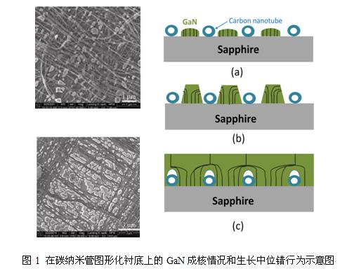
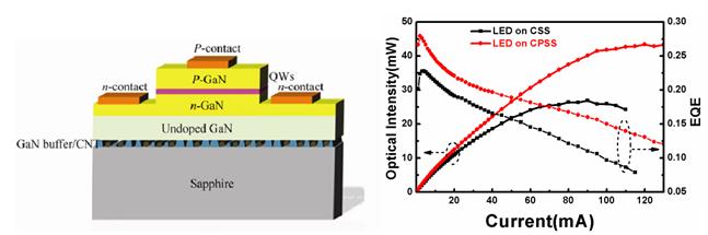
GaN material and related LED devices always suffered from the serious strains induced by the heteroepitaxy of III-N semiconductor on the most popular sapphire substrate. Although it has been optimized by many groups in the world, the prevailing dislocation density in this epilayer was of the order in 109cm-2. Taking advantage of carbon nanotubes’ super alignment on sapphire, a group from school of physics in Peking Universitycooperating with Tsinghua University, announced a novel carbon nanotube patterned sapphire substrate (CPSS). This specified CPSS was utilized for the growth of high quality GaN material and LED by MOVPE, achievingthe nano-scale mask function in epitaxy. Their results were published on Nano Research, 2012, 5(9): 646–653 和CrystEngComm. 2012, 14, 4728–4731。 Carbon nanotube patterned sapphire substrate has been fabricated by coating super-aligned CNTs on 2-inch sapphire. GaN material and related LED devices were grown by MOVPE on CPSS. Crystalline and strain in epilayers were analyzed with the equipment atBSRF. Approximation of edge dislocation density shows that the value on CPSSwas reduced to less than 25% (about 4.7×108 cm-2) accompanying with reduction of screw dislocations. The intrinsic property of dislocations in GaN on CPSS was examined by cross sectional TEM images. Numerous voids were observed at the interface between sapphire and GaN upon the carbon nanotubes.Dislocations bended around the voids and annihilated if they got contrary burgers vectors, indicating the filtering of dislocation by this CPSS. E2H mode Raman spectrummapping confirmed the change of strain in GaN layers. The stress ranging from 0.15GPa to 0.40GPa is obtained for GaN epilayer on CPSS, which is much smaller than that on conventional sapphire substrate as nearly unchanged at 0.90GPa. Although the macro stress distribution is uniform in GaN on CPSS, a pattern character of stress distribution is apparently observed. When collating the strain distribution with CNTs bundles pattern, it is found that the strain reduced most over CNT bundles, confirming the dislocation behavior around carbon nanotubes. Comparing the luminous intensity dependence on the current of LED on CPSS and conventional sapphire substrate, it is found that LEDs on CPSS not only exhibitedenhancement of luminous intensity, butalso elevated about 50%-60% saturation current and optical power. The saturation of LED performance comes from thermal sinking during operation. Superior thermal conduction of CNTs increases LED’s current capacitance significantly, guaranteed the promising future of this substrate in high power device fabrication. Carbon nanotube has chemical inertness, superior thermal and electrical conduction, and is also easily to be composed into large-size aligned nano structures. Moreover, it is environment friendly, and cheap enough that one meter long CNT array just consumes CNT film in 1 millimeter thickness. This work will open a new route for the application of carbon nanotubes.
Fig. 1:Sketch of GaN nucleation and dislocation behavior during growth on CPSS
Fig. 2: LED diagram on CPSS with its L-I and EQE curve
Article: [1] Hao Long, Yang Wei, Tongjun Yu*, Zhe Wang, Chuanyu Jia, Zhijian Yang, Guoyi Zhang, Shoushan Fan*, Modulating lateral strain in GaN-based epitaxial layers by patterning sapphire substrates with aligned carbon nanotube films. Nano Research, 5(9): 646–653, 2012. [2] Hao Long,Yang Wei,Tongjun Yu,*Zhe Wang,Chuanyu Jia, Zhijian Yang, Guoyi Zhangand Shoushan Fan*,High Quality GaNepilayers Grown on Carbon Nanotubes Patterned Sapphire Substrate by metal organic vapor phase epitaxy. CrystEngComm., 14, 4728–4731, 2012. |
|
|
| Chinese
Science Highlights
Home /

Copyright © 2011 - 2012 Beijing Synchrotron Radiation Facility