
| A stable solution-processed polymer semiconductor with record high-mobility for printed transistors |
| From: PublishDate:2013-06-15 Hits: |
Microelectronic circuits/arrays produced via high-speed printing instead of traditional photolithographic processes offer an appealing approach to creating the long-sought after, low-cost, large-area flexible electronics. Foremost among critical enablers to propel this paradigm shift in manufacturing is a stable, solution-processable, high-performance semiconductor for printing functionally capable thin-film transistors—fundamental building blocks of microelectronics. Recently, researchers in Key Laboratory of Organic Solids, Institute of Chemistry, Chinese Academy of Sciences have made great progress in this field. They report the processing and optimisation of solution-processable polymer semiconductors for thin-film transistors, demonstrating very high field-effect mobility, high on/off ratio, and excellent shelf-life and operating stabilities under ambient conditions. Exceptionally high-gain inverters and functional ring oscillator devices on flexible substrates have been demonstrated. This optimised polymer semiconductor represents a significant progress in semiconductor development, dispelling prevalent skepticism surrounding practical usability of organic semiconductors for high-performance microelectronic devices, opening up application opportunities hitherto functionally or economically inaccessible with silicon technologies, and providing an excellent structural framework for fundamental studies of charge transport in organic systems.
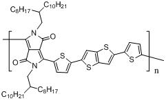
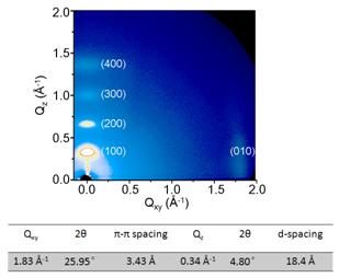
Figure 1. Chemical structures of the polymer. Tapping-mode atomic force microscopy (AFM) of a thin film of high-molecular weight sample (Mn/Mw=110,000/501,000) of the polymer showed large fibrous crystalline domain structures having dimensions of 30~40 nm in width and more than 1 μm in length. This was collaborated by the grazing incidence X-ray diffraction (GIXRD) results showing high crystallinity. The out-of-plane (Qz) diffraction exhibited a progression of peaks at Qz=0.34 Å-1 (2θ=4.80°), demonstrating an interlayer spacing of 18.4 Å. This is in excellent agreement with the calculated intermolecular polymer chain packing distance of approximately 18.5 Å for 1 with the longest chains fully extended from the backbone in a lamellar-like structure. The in-plane diffraction (Qxy) displayed a diffraction peak at Qxy=1.83 Å-1 (2θ=25.95°), demonstrating a very close π-π stacking distance of 3.43 Å. The out-of plane diffraction peaks increased significantly with increasing molecular weight (Fig. 2j, film thickness ,100 nm), attesting to a much higher crystallinity in the higher molecular weight films.
Figure 2. Grazing incidence X-ray diffraction (GIXRD) measurements of high-molecular weight polymer semiconductor (Mn/Mw = 110,100/500,700). The result was published in SCIENTIFIC REPORTS.
Article: Li J, Zhao Y, Tan HS, Guo Y, Di CA, Yu G, Liu Y, Lin M, Lim SH, Zhou Y, Su H, Ong BS.. A stable solution-processed polymer semiconductor with record high-mobility for printed transistors. Sci. Rep. 2, doi:10.1038/srep00754, 2012. |
|
|
| Chinese
Science Highlights
Home /

Copyright © 2011 - 2012 Beijing Synchrotron Radiation Facility