
| Thin Film with Insulating Interior but Metallic Surfaces |
| From: PublishDate:2013-06-15 Hits: |
With decreasing dimension, materials exhibit properties which bulk materials do not have. These properties and their related phenomena have attracted more and more attention nowadays. From the 1960s, bismuth (Bi) has drawn great interest for its low carrier concentration, small effective carrier mass and large Fermi wavelength. With the given special properties of bulk Bi, one of the interesting and appealing problems is to manipulate its electronic structure in thin films to switch Bi from a semimetal to an insulator or semiconductor by the quantum size effect. Although there have been considerable efforts in electrical conductance and Hall transport as well as Angle Resolved Photoemission Spectroscopy, the existence of semimetal-semiconductor transition in Bi films remains elusive for the results introduced even more controversies and puzzles.
FIG. 1 (a) RHEED patterns of 6 and 25 nm of Bi on BaF2; the incident electron beam is along the [11-2] direction of BaF2. (b), (c) The grazing angle XRD spectra of the same samples; the small peak around 41 degree comes from the(0-22) diffraction of the BaF2 substrate. In this letter, bismuth single crystalline films were epitaxially grown on BaF2 by MBE. To have better calibration of the sample quality, aside from the in-situ RHEED, we used Grazing angle XRD in Beijing Synchrotron Radiation Laboratory Institute of High Energy Physics. As shown in Fig. 1, we determined the structure of Bi thin film undergoes a transition from pseudocubic ((100) peak at 27.1 degree) to hexagonal ((1100) peak at 39.7 degree) phase. and also the stages of the growing process. In addition, the conductance measurement (Fig. 2(a)) showed consistent results with the RHEED and XRD experiments and we therefore conclude that we can obtain experimentally pure Bi(111) single crystal films thicker than 15 nm on BaF2(111).
FIG. 2 (a) Conductance as a function of the sample thickness at 300, 100, and 5 K. (b) Conductivity of the film interior derived from the slops of the conductance-thickness lines in region (III) of (a) as a function of temperature. The curve is an exponential fitting. The dependence of Bi films’conductance on thickness at different temperature shows that it is dominated by interior and surface at high and low temperature respectively. By plot the slops of the conductance-thickness against temperature as shown in Fig. 2(b), we proved the existence of semiconductor phase in thin bismuth films. This gives a strong argument to the long studied and debated problem.
FIG. 3 (a) Conductivity-temperature curves (540–60 nm from top to bottom) normalized with the value at 300 K. The inset is a zoom-in from 270 to 300 K. (b) The temperature coefficients of conductivity between 270 and 300 K as a function of sample thicknesses. The black curve is a guide to the eye.
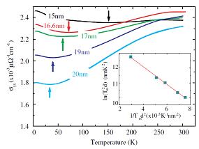
FIG.4 Temperature dependent conductivities of samples with different thickness. The arrows marke the minimal points. Further, we determined the semimetal-to-semiconductor transition point by studying the temperature coefficients of conductivity’s dependence on temperature. Base on our understanding that bismuth films’s transport properties are the joint effect of metallic surface state and semiconductor interior, we made a model to study the widely observed yet perplexing behaviors in the conductivity of bismuth films. We proved quantitatively that these behaviors are the results of competition between the two components in the Bi films.
Article: Xiao, S., Wei, D. & Jin, X. Bi(111) Thin Film with Insulating Interior but Metallic Surfaces. Physical Review Letters 109, 166805, doi:10.1103/PhysRevLett.109.166805 (2012). |
|
|
| Chinese
Science Highlights
Home /


Copyright © 2011 - 2012 Beijing Synchrotron Radiation Facility